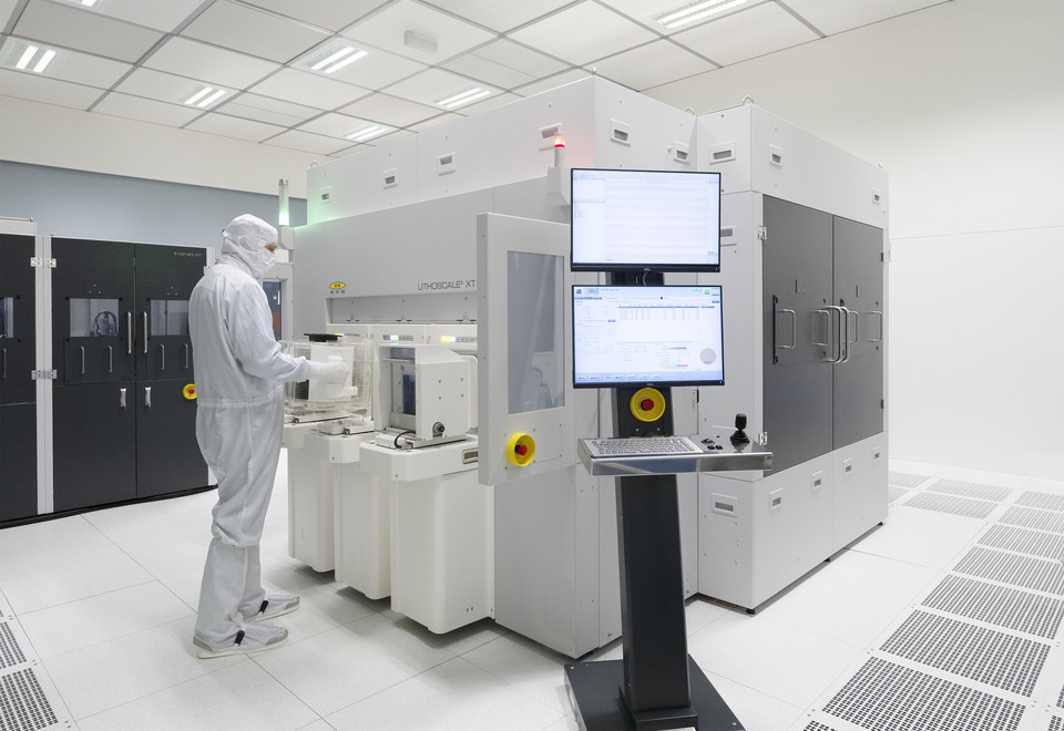
EV Group(EVG) introduced the LITHOSCALE XT maskless exposure(MLE) system, the industry's first true high-throughput/high-resolution digital lithography solution for high-volume-manufacturing(HVM) heterogeneous integration applications.
With a new dual-stage design, up to six exposure units, a dual-wavelength direct laser source as well as additional hardware and software enhancements, the LITHOSCALE XT offers up to a five-fold increase in throughput compared to EVG's current-generation LITHOSCALE solution, which previously was the highest-throughput maskless lithography system at comparable resolution.
The LITHOSCALE XT is ideally suited for applications involving multi-die patterning, fan-out wafer-level packaging(FoWLP) for AI and high-performance computing(HPC) devices, panel-level packaging, MEMS, advanced imaging sensors, and die traceability for security and automotive applications.
Heterogeneous integration—the manufacturing, vertical assembly and packaging of multiple different dies into a single package—has led to greater package complexity, as well as a greater number of package options available. This in turn is driving the need for greater design flexibility and the ability to adopt both die-level and wafer-level designs simultaneously in back-end lithography.
Accurate reconstitution of wafers is a key parameter in integrating dies from various wafer fabs or fab lines in multi-die solutions. Steppers and other mask-based patterning systems struggle to cope with inaccuracies from die-placement and die-shift variations caused by over-molding.
In addition, the reticle size and optics dimensions of static exposure systems limit the exposure area. This is particularly challenging in large die interposer fabrications, where stitch-lines and/or mismatches overlap regions of the reticle exposure field, which can affect the electrical properties within the redistribution layer(RDL).
The ability to generate a homogenous pattern for interposers that exceed current reticle size is crucial for devices with complex designs, such as those used in advanced graphic processing, 5G, AI and HPC.
“The adoption and evolution of heterogeneous integration is driving tighter performance requirements for back-end lithography that can no longer be fully met with traditional mask-based solutions like steppers and mask aligners. While the technical advantages of MLE technology are abundantly clear, throughput has been a barrier to HVM adoption until now,” said Dr. Bernhard Thallner, pathfinding and optics director at EVG
“Our newest MLE platform, LITHOSCALE XT, supports our customers' unique patterning needs in HVM, not only for advanced packaging but also numerous other applications that can benefit from its combination of high versatility, resolution and throughput. We are ready to engage with customers and partners to help them leverage the myriad benefits of our MLE technology for their respective unique manufacturing needs.”
관련기사
- Penguin Solutions Announces New Altus HPC Servers with AMD EPYC 9005
- DNP Accelerates Development of Photomask Manufacturing Process
- EVG Completes Construction of New Manufacturing V Building
- Rescale Accelerates Enterprise HPC with Two Key Executive Appointments
- Yield Engineering Systems Delivers Multiple VertaCure LX Systems
- EUV Tech Expands Global Footprint with Opening of First International Office in Singapore