Toshiba Europe Ltd announced it has developed the world’s first chip-based quantum key distribution(QKD) system. This advance will enable the mass manufacture of quantum security technology, bringing its application to a much wider range of scenarios including to Internet of Things(IoT) solutions.
QKD addresses the demand for cryptography which will remain secure from attack by the supercomputers of tomorrow. In particular, a large-scale quantum computer will be able to efficiently solve the difficult mathematical problems that are the basis of the public key cryptography widely used today for secure communications and e-commerce.
In contrast, the protocols used for quantum cryptography can be proven secure from first principles and will not be vulnerable to attack by a quantum computer, or indeed any computer in the future.
The QKD market is expected to grow to approximately $20 billion worldwide in FY20351. Large quantum-secured fibre networks are currently under construction in Europe and South-East Asia, and there are plans to launch satellites that can extend the networks to a global scale. In October 2020,
Toshiba released two products for fibre-based QKD, which are based on discrete optical components. Together with project partners, Toshiba has implemented quantum-secured metro networks and long-distance fibre optic backbone links in the UK, Europe, US and Japan.
For quantum cryptography to become as ubiquitous as the algorithmic cryptography we use today, it is important that the size, weight and power consumption are further reduced.
This is especially true for extending QKD and quantum random number generators(QRNG) into new domains such as the last-mile connection to the customer or IoT. The development of chip-based solutions is essential to enabling mass market applications, which will be integral to the realisation of a quantum-ready economy.
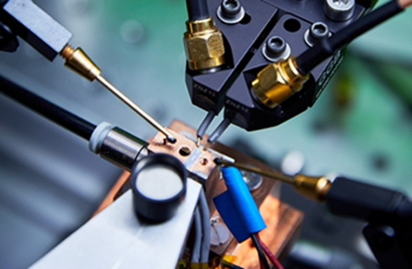
Toshiba has developed techniques for shrinking the optical circuits used for QKD and QRNG into tiny semiconductor chips. These are not only much smaller and lighter than their fibre optic counterparts, but also consume less power.
Most significantly, many can be fabricated in parallel on the same semiconductor wafer using standard techniques used within the semiconductor industry, allowing them to be manufactured in much larger numbers. For example, the quantum transmitter chips developed by Toshiba measure just 2x6mm, allowing several hundred chips to be produced simultaneously on a wafer.
“Photonic integration will allow us to manufacture quantum security devices in volume in a highly repeatable fashion. It will enable the production of quantum products in a smaller form factor, and subsequently allow the roll out of QKD into a larger fraction of the telecom and datacom network.” said Andrew Shields, Head of Quantum Technology at Toshiba Europe.
관련기사
- Toshiba releases ARM Cortex-M4 MCU for Motor Control
- KIOXIA Announces Industry’s First 512GB Automotive UFS
- Toshiba Announces Full Availability of dynaEdge AR Smart Glasses
- TSMC Recognizes Partners of the Year at 2021 OIP Ecosystem Forum
- TCL Mini LED TV Disrupts Gaming Experience with AMD FreeSync
- New EAGLEi Carrier Inspection Technology Center Established
- Nanotronics Unveils New nSpec Macro Standalone System
- Navitas Announces Availability of GaN power ICs for Data Center and EV
- NTT has developed an Optical Fiber-Coupled Quantum Light Source
- IQM’s Quantum Fabrication Facility Gets a €35 Million Boost From the EIB